Analog To Digital Converter Design
Undergraduate Project
Principal Supervisors
- Prof. Tharmarajah Thiruvaran
Group Members
- Indusan Senavirathna
- Thirunamam Thapothanan
- Sayalolibavan Vithurshan
The project involved designing and implementing an A/D converter with specific requirements. The goal was to achieve a bandwidth of 0-100Hz, 6 levels of uniform quantization, and minimize aliasing noise while avoiding distortion or attenuation within the interested bandwidth. The project used a TMS6713 DSP development board to generate input sinusoidal signals and included the design of an amplifier with offset to achieve a peak-to-peak signal range of 0-6V.
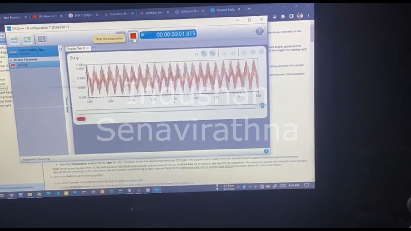
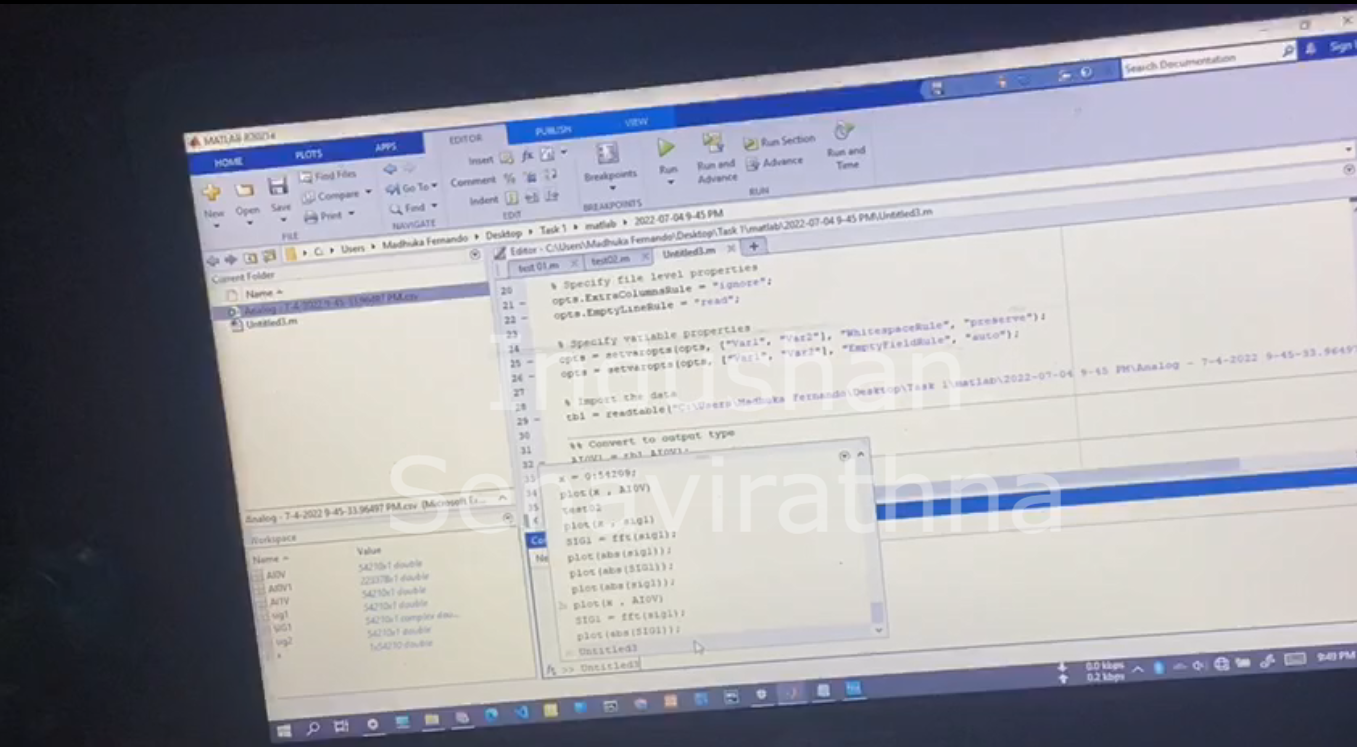
The encoder was not built, but the quantized output signal was captured using DAQ for spectrum display in MATLAB. The project also required demonstrating the system by displaying the quantized output signal and sampled signal on an oscilloscope.
Throughout the project, knowledge of electronic components such as MOSFETs, operational amplifiers, and capacitors was applied. The researcher gained familiarity with oscilloscopes and signal generators and learned how to generate and assess waveforms. Filter design was explored, including types like Butterworth, Chebyshev, and Bessel, taking into account cutoff and stop band frequencies. The sampling and hold circuit's operation and the selection of suitable capacitors based on the sample frequency were studied. Comparators were constructed using op-amps to quantize the filter output.
While facing challenges during the lab work, issues with achieving the minimum sampling frequency, non-availability of exact capacitor and resistor values, variations in cutoff and stop band frequencies, and distortion of the output waveform were encountered. These problems were addressed by designing a high-order Butterworth filter, using approximate values for capacitors and resistors available in the laboratory, considering the resistance added by connecting wires, and supplying the gate of the MOSFET with a clock signal slightly higher than the input signal. Additionally, a suitable capacitor was used to ensure correct charging and holding voltage.
Overall, the project involved designing and implementing an A/D converter while overcoming various challenges related to circuitry, filtering, and signal processing to achieve the desired specifications and minimize distortions.
- Designed and implemented an A/D converter: The project involved designing and constructing an analog-to-digital converter (A/D converter) capable of converting analog signals into digital form. The converter was specifically designed to meet the project requirements.
- Achieved bandwidth and quantization requirements: The A/D converter was designed to operate within a bandwidth of 0-100Hz. It ensured that the input signals falling within this range were accurately quantized using a uniform quantization scheme with 6 levels. This allowed for the faithful representation of analog signals in digital form.
- Minimized aliasing noise: Special consideration was given to minimizing aliasing noise during the conversion process. Aliasing noise refers to the distortion introduced when a signal is improperly sampled. By carefully designing the converter and incorporating appropriate filtering techniques, aliasing noise was minimized to ensure the fidelity of the digital representation of the input signal.
- Minimized distortion and attenuation: To maintain the integrity of signals within the interested bandwidth, efforts were made to minimize distortion and attenuation. Distortion refers to any alterations or changes in the shape or characteristics of the input signal, while attenuation refers to the reduction in signal strength. The design of the A/D converter focused on minimizing both distortion and attenuation to ensure accurate representation of the input signal.
- Designed amplifier with offset: An amplifier with offset was specifically designed to accommodate the input signal's peak-to-peak range of 0-6V. The amplifier helped amplify the input signal and introduce an offset to achieve the desired peak-to-peak range for accurate conversion.
- Generated input sinusoidal signals: Using the TMS6713 DSP development board, the project required generating input sinusoidal signals for testing and demonstration purposes. The board was utilized to produce the requested signals, including the primary signal of interest and any additional noise signals.
- Captured quantized output signal using DAQ: The quantized output signal, resulting from the A/D conversion process, was captured using a data acquisition (DAQ) system. The DAQ system allowed for the digital signal to be recorded and further analyzed using MATLAB.
- Demonstrated the system using an oscilloscope: The A/D converter system was demonstrated by displaying the quantized output signal, which represented the continuous-time digital signal, and the sampled signal on an oscilloscope screen. This demonstration showcased the real-time performance and accuracy of the converter system.
Skills
- Understanding of electronic components, including MOSFETs, operational amplifiers, and capacitors.
- Familiarity with oscilloscopes and signal generators for waveform analysis and manipulation.
- Filter design, including knowledge of Butterworth, Chebyshev, and Bessel filters.
- Signal quantization using comparators constructed with operational amplifiers.
- Experience with the TMS6713 DSP development board for generating input sinusoidal signals.
- Design and implementation of an amplifier with offset to achieve a specific peak-to-peak signal range.
- Data acquisition using DAQ (Data Acquisition) to capture the quantized output signal.
- Signal spectrum analysis in MATLAB.
- Troubleshooting and problem-solving in circuit design and implementation.
- Utilizing various technologies, such as MOSFETs for signal routing, operational amplifiers for signal processing, and capacitors for filtering and timing.
- Knowledge and application of analog and digital signal processing techniques.
- Understanding of sampling and hold circuits.
- Familiarity with RC time constants and their impact on signal behavior.
- Hands-on experience with circuitry and wiring, including consideration of resistance introduced by connecting wires.
- Application of patience and perseverance in dealing with complex circuits and system integration.